
Tofu is a simple relay-switching circuit simulator. Electronic components and their connections are described in text files and fed into Tofu for simulation. This tutorial discusses relay circuit theory and how to use the Tofu circuit simulator.
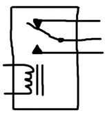
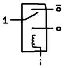
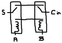
A relay consists of a solenoid (an electromagnetic) and a 3-contact switch. Two of the contacts of the switch are stationary. The third contact is a mechanical lever that can toggle between the other two. A spring applies tension to the lever and holds 2 of the contacts together in the relay’s relaxed position. However, when the solenoid is energized, it magnetically draws the lever, overcoming the tension of the spring, and moves it from one stationary contact to the other. When the solenoid is shutoff, the spring toggles the switch back to the initial state.
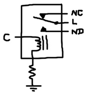
A relay physically has 5 terminals, but we can connect 1 end of the solenoid to a resistor and connect the resistor to ground. This produces a component with 4 logical terminals: coil (C), lever (L), normally-disconnected (ND) and normally-connected (NC). To energize the solenoid, terminal C must be connected to the power voltage.
Power indicates a logical true, the binary 1. Lack of power indicates a logical false, the binary 0. Note, 0 is not the ground voltage. Rather, 0 means floating.
run CommandThe run command accepts the following parameters:
run [simulation iterations] [half clock period] [component] [[ ... component parameters ... ]]
Here’s a 1 line Tofu file example:
run 3 1 r 1 1 ? ?
The first parameter indicates that the simulation will terminate after 3 iterations. Each iteration consists of 2 phases. In the first phase, the power voltage propagates from the power node through the electronic components successively energizing nodes along the way. If a circuit pathway exists between the power node and some other node, that node is energized and is said to be “reachable” from the power node. Unreachable nodes are left floating; they are not connected to power or ground. At the end of the first phase, reachable nodes are assigned logic 1 and unreachable nodes are assigned logic 0. In the second phase, the internal states of the electronic components change in response to nodes they are connected to. In the case of a relay, that means the lever may flip position in response to the coil node value.
If you specify 0 for the iteration count, the simulation will continue indefinitely.
The second parameter is the half clock period. This is discussed further below.
The third parameter, r, instructs Tofu to instantiate a relay. Relays accept the 4 nodes discussed above: coil, lever, normally-disconnected and normally-connected. When the coil node is 0, the lever and the normally-connected nodes form a conductive pathway. When the coil node is 1, the lever and normally-disconnected nodes form a conductive pathway. One way to think about is like this:
r booleanNode leverNode trueNode falseNode

if (booleanNode) { leverNode <-> trueNode } else { leverNode <-> falseNode }
The two 1’s indicate that the coil and lever nodes are connected to power. The ?’s are probes, nodes we want to inspect during the simulation. Since the relay starts off in its relaxed position (lever and normally-connected touching) and the coil node is connected to power, the lever moves between contacts. Here’s the output:
Build complete: 1 components, 2 nodes.
1: 01
2: 10
In the first iteration, the normally-disconnected node was floating (0) and the normally-connected node was energized (1) because of the position of the lever. However, in the second iteration, the lever moved and the values swapped as a result. Even though we asked for 3 iterations, only 2 printed out. Tofu won’t display iterations unless a probed node changes state.
Here’s a variation of the example:
run 100 10 r c 1 ? ?
In this case, we ask for 100 iterations with a clock period of 20 (the clock will change every 10 iterations). Tofu provides the clock node, c, and the inverse clock node, k. The clock node will flip between power (1) and floating (0) at the specific iteration count. The inverse clock node, as it’s name suggests, is always the negative of the clock node value. In this example, the coil node is specified as the clock. Every 10 iterations, the lever will toggle. Here’s the result:
Build complete: 1 components, 2 nodes.
1: 01
2: 10
11: 01
21: 10
31: 01
41: 10
51: 01
61: 10
71: 01
81: 10
91: 01
The run command can be placed anywhere within the Tofu file. Typically, it’s the first or the last statement.
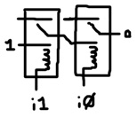
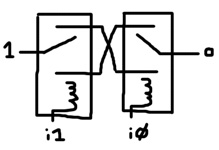
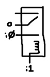
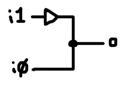
def CommandTofu allows you to define components composed other components with the def command. The image below shows how to construct a buffer out of a single relay and the symbol for a buffer.
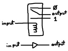
A buffer simply propagates the value of the input node to the output node, but after a short delay. The lever takes an iteration to flip in response to a change in input. Again, the 0 and 1 refer to floating (connected to nothing as opposed to ground) and power respectively. Here’s how to define a buffer:
# Buffer
def buf input output :
  r input output 1 0

run 100 10 buf c ?
# is used to indicate comments. The # and any characters to the right of the # are ignored by Tofu.
The form of the def command is:
def [component name] [[ ... component node names ... ]] :
The subcomponents follow. Indentation is ignored, but recommended. A component definition is terminated by the start of another component definition (when another def command is reached), a run command is reached or the end of the file is reached. In this case, run ends the definition of buf. As per the last example, we request 100 iterations with a clock period of 20. The clock node is used as the input node and we probe the output node. Here’s the result:
Build complete: 1 components, 2 nodes.
1: 0
2: 1
11: 0
21: 1
31: 0
41: 1
51: 0
61: 1
71: 0
81: 1
91: 0
How about an inverter?
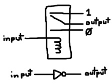
# Inverter
def inv input output :
  r input output 0 1

run 100 10 inv c ?
Result:
Build complete: 1 components, 2 nodes.
1: 1
2: 0
11: 1
21: 0
31: 1
41: 0
51: 1
61: 0
71: 1
81: 0
91: 1
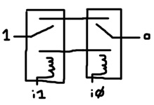
Using a single relay, it’s actually possible to produce a buffered and an inverted signal:
Here’s the definition followed by some tests:
def bufInv input output outputNeg :
  r input 1 output outputNeg

run 10 1 bufInv 0 ? ?

Build complete: 1 components, 3 nodes.
1: 01

run 10 1 bufInv 1 ? ?

Build complete: 1 components, 2 nodes.
1: 01
2: 10
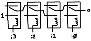
Many different kinds of relays exist, but the relay depicted here is the only kind provided by Tofu. One useful type of relay contains 1 coil and multiple switches like this four double-pole relay:
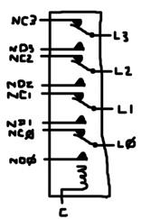
# Four double-pole relay
def r4 coil l3 nd3 nc3 l2 nd2 nc2 l1 nd1 nc1 l0 nd0 nc0 :
  r coil l3 nd3 nc3
  r coil l2 nd2 nc2
  r coil l1 nd1 nc1
  r coil l0 nd0 nc0

run 100 10 r4 c 1 ? ? 1 ? ? 1 ? ? 1 ? ?
The new component, r4, is an abstraction that represents the four double-pole relay. If you choose, after defining it, you can ignore r and build all circuits completely out of r4. Here’s the output:
Build complete: 4 components, 8 nodes.
1: 01010101
2: 10101010
11: 01010101
21: 10101010
31: 01010101
41: 10101010
51: 01010101
61: 10101010
71: 01010101
81: 10101010
91: 01010101
Note, in the definition of r4, it’s tempting to use c for the coil node, but c is reserved for the clock node. Nodes can’t share names with keywords (def and run), reserved node names (c, k, 0 and 1) and components (r and others you define). Node names can be numerical, but 0 and 1 are already taken.
An AND gate is produced by chaining relays in series. The inputs are the coil nodes. The outputs are the levers. The normally-disconnected node of the first relay in the chain is connected to power. Each lever node is successively connected to the normally-disconnected node of the next relay in the chain. In this way, all levers must be flipped for the output to be 1.
# AND Gate
def and i1 i0 o :
  r i0 z 1 0
  r i1 o z 0
Note that the node z is not one of the nodes in the def argument list. It exists only within the scope of the AND gate definition like a local variable.
The series chain can be extended to any number of inputs. Here’s a 4-input AND gate:
# 4-Input AND Gate
def and4 i3 i2 i1 i0 o :
  r i3 z 1 0
  r i2 y z 0
  r i1 x y 0
  r i0 o x 0
One interesting thing to note is that no matter how long the chain is, it always takes the same number of iterations to generate the output because all the relay levers flip in parallel.
A relay series chain can be thought of as a pattern detector. The 4-input AND gate only produces a 1 signal if it detects the pattern 1111. To detect an arbitrary pattern you simply need to adjust the wiring on those relays that look for 0’s. For instance, this circuit detects the pattern 1010:
# 1010 Pattern Detector
def 1010detector i3 i2 i1 i0 o :
  r i3 z 1 0
  r i2 y 0 z
  r i1 x y 0
  r i0 o 0 x
A NAND gate only produces an output of 0 if all inputs are 1. This is done by putting relays in parallel. The inputs are connected to the coils and the output is shared among all the normally-connected nodes. The levers are connected to power. All the levers need to be flipped to prevent power from reaching the output node.
# NAND Gate
def nand i0 i1 o :
  r i0 1 0 o
  r i1 1 0 o
The OR gate is very similar to NAND. The relays are put in parallel with the inputs connected to the coils. The levers are connected to power, but the normally-disconnected nodes are joined together to form the output. In this way, if any of the levers are flipped, power will reach the output node. The similarity to NAND follows from De Morgan’s Law: A | B = !(!A & !B). Also note that an OR gate is essentially a bunch of buffers connected in parallel.
# OR Gate
def or i0 i1 o :
  r i0 1 o 0
  r i1 1 o 0
NOR is very similar to AND. The relays are chained in series forming a path from power through the levers and the normally-connected nodes. The inputs are the coils. If any of the levers are flipped, the chain will be broken. All inputs need to be 0 for the output to be 1. NOR can be thought of as a pattern detector looking for all zeros (a zero detector). The similarity to AND follows from De Morgan’s Law: !(A | B) = !A & !B.
# NOR Gate
def nor i0 i1 o :
  r i0 1 0 z
  r i1 z 0 o
XOR (exclusive-OR) produces an output of 1 only if the inputs don’t match. This is achieved by connecting both inputs to the coils. One lever is connected to power and the other lever is the output. The normally-connected and normally disconnected terminals of the relays are cross connected. A pathway only exists from one lever to the other if they are in opposite states.
# XOR Gate
def xor i0 i1 o :
  r i0 1 b a
  r i1 o a b
XNOR is the inverse of XOR. It only produces an output of 1 if the inputs match. The circuit is the same as XOR except there is no cross connection. A pathway only exists from one lever to the other if the levers are in the same state.
# XNOR Gate
def xnor i0 i1 o :
  r i0 1 a b
  r i1 o a b
If you were actually constructing a computing device out of relays, you’d probably want to use as few as possible. Consider constructing a 2-input AND gate with a single relay:
# AND Gate with Single Relay
def and1 i1 i0 o :
  r i1 o i0 0
If you test it, it will certainly appear to work; however, this circuit is dangerous. Up until now, inputs were always connected to the coils of the relays. Meaning, the output was fully decoupled from the input. There was no way a signal could inadvertently propagate from the output back to one of the inputs. The coil is simply not connected to any of the other terminals of the relay. But, in this circuit, if node i1 were energized and the output node were energized by some other circuitry that it’s connected to, node i0 could get energized. Power can flow in this AND gate in reverse. If you use this optimization, you must take that possibility into consideration.
How about an OR gate with no relays at all?
This circuit poses the same danger as the AND optimization. Since the inputs are connected to each other, one could inadvertently energize the other. Here’s a 1-relay version that’s a little safer:
Now at least one of the inputs is decoupled from the output by a buffer. There’s still the possibility of the output driving the other input. Note, if you use 2 buffers, the circuit is equivalent to the OR gate presented in the previous section.
Given single-bit numbers, A and B, what is A + B? There’s only 4 combinations:
0 + 0 = 00
0 + 1 = 01
1 + 0 = 01
1 + 1 = 10
The sum of 2 single-bit numbers is a 2-bit number containing a sum bit and a carry bit. Here’s a truth table to make it clearer:
AB S1 S0
00  0  0
01  0  1
10  0  1
11  1  0
S0 can be generated with an XOR gate and S1 can be generated with an AND gate. Combining those gates together produces what is known as a “half adder”:
# Half Adder
def halfAdder a b s1 s0 :
  and a b s1
  xor a b s0
Note, S0 and S1 were used as symbols instead of S and C for the sum and carry bits respectively because we’ll built up to multi-bit adders below and also, C is reserved for the clock node.
Given 3 single-bit numbers, A, B, and C, what is A + B + C? If all 3 inputs are 1, the result is 11 in binary. So, we still only need 2 output bits. We can start out by adding A and B with the half adder to produce the 2-digit number S1 S0. Then we’ll add C to that 2-digit number. To do so, we’ll add S0 and C with another half adder. That will produce a sum bit, which is the lower bit in the final answer, and a carry which must be added to S1 to produce the higher bit in the final answer. That suggests we need 3 half adders, but consider possible carry combinations here. If S1 is 1, then S0 must be 0 from the table above. In that case, adding S0 and C produces no carry. If S1 is 0, then adding S0 and C may produce a carry, which will become the higher bit in the final answer. So, instead of a third half adder, the higher bit in the final answer can be produced by ORing together S1 and the carry produced by adding S0 and C.
So, what good is such a circuit anyway? The idea is to produce a circuit called a “full adder” that takes 2 single-bit numbers, A and B, and third single-bit number, carry-in, and produce a sum bit and a carry-out bit. The full adders will be chained together by connecting the carry-in and carry-out terminals together. The initial carry-in will be set to 0. The final carry-out is the carry produced by adding together the multi-bit input values. Here’s the full adder:
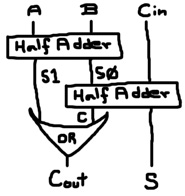
# Full Adder
def fullAdder carryIn a b carryOut sum :
  halfAdder a b s1 s0
  halfAdder s0 carryIn carry sum
  or s1 carry carryOut
Now, let’s chain them together to produce multi-bit adders:
# 2-bit Adder
def adder2 carryIn a1 a0 b1 b0 carryOut s1 s0 :
  fullAdder carryIn a0 b0 carry s0
  fullAdder carry a1 b1 carryOut s1

# 4-bit Adder
def adder4 carryIn a3 a2 a1 a0 b3 b2 b1 b0 carryOut s3 s2 s1 s0 :
  adder2 carryIn a1 a0 b1 b0 carry s1 s0
  adder2 carry a3 a2 b3 b2 carryOut s3 s2

# 8-bit Adder
def adder8 carryIn
             a7 a6 a5 a4 a3 a2 a1 a0
             b7 b6 b5 b4 b3 b2 b1 b0
    carryOut s7 s6 s5 s4 s3 s2 s1 s0 :
  adder4 carryIn a3 a2 a1 a0 b3 b2 b1 b0 carry s3 s2 s1 s0
  adder4 carry a7 a6 a5 a4 b7 b6 b5 b4 carryOut s7 s6 s5 s4
There are a few things you should note from this. First, you can break up long lines with carriage returns. The parser uses the colon to determine when the def parameter list ends. For the body of def, the parser uses the lengths of the parameter lists of the defined electronic components to determine when a node list ends. Unfortunately, this means that you can only use electronic components that were defined above it. Meaning, for example, you can’t define adder2 before defining fullAdder. Second, there is no looping syntax. It would be nice to loop 8 times, connecting full adders together to produce adder8. Instead, doubling components up is used.
Let’s test out our 8-bit adder. Let’s compute 57 + 142, which is 111001 + 10001110 in binary:
# 57 + 142 = ?
run 100 1 adder8 0
    0 0 1 1 1 0 0 1
    1 0 0 0 1 1 1 0
  ? ? ? ? ? ? ? ? ?
Note that 0 is used for the initial carry-in. Here’s the result:
Build complete: 80 components, 145 nodes.
1: 000000000
3: 010110111
4: 010100111
6: 010000111
8: 011000111
That’s the correct answer (11000111 is 199 in decimal). This circuit is known as a “ripple adder” because the carry values must ripple from one adder to the next in the chain before the final answer is determined. That means it can take many iterations to get the answer. Consider 255 + 1. 255 is 11111111 in binary; so, we’ll produce a running carry that must travel from one end of the ripple adder to the other before it comes up with 256:
# 255 + 1 = ?
run 100 1 adder8 0
    1 1 1 1 1 1 1 1
    0 0 0 0 0 0 0 1
  ? ? ? ? ? ? ? ? ?

Build complete: 80 components, 144 nodes.
1: 000000000
3: 011111110
4: 011111100
6: 011111000
8: 011110000
10: 011100000
12: 011000000
14: 010000000
16: 000000000
17: 100000000
Konrad Zuse, the computer pioneer, came up with a better way. He proposed a dual-rail-carry full adder that uses 2 four-double-pole relays:
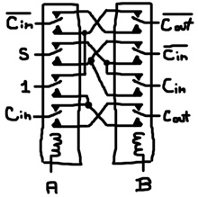
“Dual-rail-carry” means that in addition to accepting carry-in and producing carry-out, it accepts and produces the inverse carry signals. As with the full adder above, these are chained together to form a multi-bit adder. The initial carry-in is set to 0 and the initial carry-in-negative is set to 1. The final carry-out is the carry for the sum of the multi-bit input values and the final carry-out-negative is ignored.
# Konrad Zuse Dual-Rail-Carry Full Adder
def zuseFullAdder carryInNeg carryIn a b carryOutNeg carryOut sum :
  r4 a carryInNeg y z sum w x 1 v y carryIn u v
  r4 b carryOutNeg z y carryInNeg x w carryIn w x carryOut v u

# Konrad Zuse Dual-Rail-Carry 2-bit Adder
def zuseAdder2 carryInNeg carryIn a1 a0 b1 b0 carryOutNeg carryOut s1 s0 :
  zuseFullAdder carryInNeg carryIn a0 b0 cOutNeg cOut s0
  zuseFullAdder cOutNeg cOut a1 b1 carryOutNeg carryOut s1

# Konrad Zuse Dual-Rail-Carry 4-bit Adder
def zuseAdder4 carryInNeg carryIn a3 a2 a1 a0 b3 b2 b1 b0
    carryOutNeg carryOut s3 s2 s1 s0 :
  zuseAdder2 carryInNeg carryIn a1 a0 b1 b0 cOutNeg cOut s1 s0
  zuseAdder2 cOutNeg cOut a3 a2 b3 b2 carryOutNeg carryOut s3 s2

# Konrad Zuse Dual-Rail-Carry 8-bit Adder
def zuseAdder8 carryInNeg carryIn
                         a7 a6 a5 a4 a3 a2 a1 a0
                         b7 b6 b5 b4 b3 b2 b1 b0
    carryOutNeg carryOut s7 s6 s5 s4 s3 s2 s1 s0 :
  zuseAdder4 carryInNeg carryIn a3 a2 a1 a0 b3 b2 b1 b0 cOutNeg cOut s3 s2 s1 s0
  zuseAdder4 cOutNeg cOut a7 a6 a5 a4 b7 b6 b5 b4
      carryOutNeg carryOut s7 s6 s5 s4
Note, r4 is defined above; it’s not a standard component. Now, let’s repeat the computations above:
# 57 + 142 = ?
run 100 1 zuseAdder8 1 0
    0 0 1 1 1 0 0 1
    1 0 0 0 1 1 1 0
? ? ? ? ? ? ? ? ? ?

Build complete: 64 components, 81 nodes.
1: 1000000000
2: 1011000111

# 255 + 1 = ?
run 100 1 zuseAdder8 1 0
      1 1 1 1 1 1 1 1
      0 0 0 0 0 0 0 1
  ? ? ? ? ? ? ? ? ? ?

Build complete: 64 components, 80 nodes.
1: 1000000000
2: 0100000000
Ignore the left-most bit; it’s the carry-out-negative. The answers are correct. Amazingly, both computations took only 2 iterations. In fact, regardless of the input values, it will always take exactly 2 iterations even if we widen this to any number of bits. How is this possible? The bits of the numbers we want to add are channeled into the relay coils. After the first iteration, all the relay levers flip in parallel. In the second iteration, the carry-in and the carry-in-negative signals propagate through the relays. The carry signals are not connected to any coils; so, no relay levers need to move in response to this propagation. Consequentially, the multi-bit sum is produced in the second iteration.
So, how did Konrad Zuse come up with this? Let’s start with the truth table:
Iiab Oos
1000 100
1001 101
1010 101
1011 010
0100 101
0101 010
0110 010
0111 011
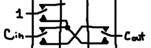
I, i, O, o are carry-in-negative, carry-in, carry-out-negative and carry-out respectively (the negatives are capitalized). If you look carefully at s, you’ll notice it’s the XOR of a and b when I is 1 and it’s the XNOR of a and b when i is 1. As described above, XOR can be created by cross-connecting 2 relays, which forces both levers to be in opposite states for a signal to be carried from one lever to the other. In this case, instead of power being that signal, carry-in-negative is the signal; so, the XOR only takes place when I is 1:
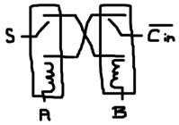
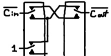
Similarly, an XNOR is constructed using carry-in instead of power; so, the XNOR only takes place when i is 1.
Taking advantage of the dangerous OR optimization discussed above, the XOR and XNOR are combined like this:
Since the carry-in and carry-in-negative levers move together, no pathway exists that allows them to touch and inadvertently energize each other. So, the optimization is okay in this case.
Returning to the truth table, o looks like OR when i is 1 and o looks like AND when i is 0. For either value of i, o is 1 when a and b are both 1. Now, the only difference between OR and XOR is the case when a and b are both 1; so, we can use XOR as long as we can force the output to 1 when a and b are both 1. That XOR will be powered by i; meaning, o will be 0 when i is 0 except when a and b are both 1. Putting those ideas together yields this part of the circuit:
The inverse circuit is built along the same lines:
What about negative numbers? These adders are already capable of handling them. In binary, a number can be interpreted as signed or unsigned where the sign bit is the left-most bit. When the sign bit is 1, it’s a negative number. Consider the example above where we added 57 and 142. 142 in binary is 10001110. This is equivalent to -114. How so? You can reverse the sign of a binary number by negating all bits and adding 1. If we negate the bits we get 01110001. And, if we add 1 to that we get 01110010, which is 114. When we computed the sum of 57 and 142, we also computed the sum of 57 and -114. The result was 11000111. This is equivalent to -57. Well, almost. If we include the carry-out bit, the result was 011000111. Carry-out represents the left-most digit of the sum. It should be 1 since the left-most digit of a negative number is 1. We’ll get back to this issue momentarily.
How about subtraction? It’s fairly straightforward to convert a multi-bit adder into a multi-bit adder/subtractor. The circuit will provide an extra input. When that input is 0, it will add A and B. When it’s 1, it will compute A – B. To subtract, the circuit will negate the bits of B, add 1 and add that total to A. To do the bitwise negation, we can’t just use inverters on the bits of B because the negation should only take place if the subtract signal is 1. The solution is to use XOR gates where one input is a bit of B and the other input is the subtract signal. If the subtract signal is 0, the B bit passes through unchanged (a number XORed against 0 is the original number). If the subtract signal is 1, the B bit is inverted. To add 1 to the bitwise negated B, we’ll use 1 as the initial carry-in instead of 0 during subtraction (i.e. connect initial carry-in to the subtract signal itself). Now, what about that pesky carry-out bit? The adder/subtractor interprets A and B as positive numbers. You can imagine that they each have an extra leading 0 bit. When B is bitwise negated, that leading bit should always turn into a 1. When the negated B plus 1 is added to A, it may produce a carry-out. If it doesn’t produce a carry-out, the negated leading bit should become the carry-out in the final answer. If a carry-out was produced, it should be added to this leading, which sums to 10 in binary. We’ll only keep the lower bit of that 2-digit value. Meaning, if we’re subtracting, we need to invert the carry-out to remain consistent with the concept of the leading bit. Again, an XOR gate comes to the rescue.
# 1-bit Partial Adder/Subtractor
def xFullAdder subtract carryInNeg carryIn a b carryOutNeg carryOut sum :
  xor subtract b bNeg
  zuseFullAdder carryInNeg carryIn a bNeg carryOutNeg carryOut sum

# 2-bit Partial Adder/Subtractor
def xFullAdder2 subtract carryInNeg carryIn
    a1 a0 b1 b0 carryOutNeg carryOut s1 s0 :
  xFullAdder subtract carryInNeg carryIn a0 b0 cOutNeg cOut s0
  xFullAdder subtract cOutNeg cOut a1 b1 carryOutNeg carryOut s1

# 4-bit Partial Adder/Subtractor
def xFullAdder4 subtract carryInNeg carryIn a3 a2 a1 a0 b3 b2 b1 b0
    carryOutNeg carryOut s3 s2 s1 s0 :
  xFullAdder2 subtract carryInNeg carryIn a1 a0 b1 b0 cOutNeg cOut s1 s0
  xFullAdder2 subtract cOutNeg cOut a3 a2 b3 b2 carryOutNeg carryOut s3 s2

# 8-bit Partial Adder/Subtractor
def xFullAdder8 subtract carryInNeg carryIn
                       a7 a6 a5 a4 a3 a2 a1 a0
                       b7 b6 b5 b4 b3 b2 b1 b0
    carryOutNeg carryOut s7 s6 s5 s4 s3 s2 s1 s0 :
  xFullAdder4 subtract carryInNeg carryIn a3 a2 a1 a0 b3 b2 b1 b0
      cOutNeg cOut s3 s2 s1 s0
  xFullAdder4 subtract cOutNeg cOut a7 a6 a5 a4 b7 b6 b5 b4
      carryOutNeg carryOut s7 s6 s5 s4

# 8-bit Adder/Subtractor
def adderSubtractor subtract
             a7 a6 a5 a4 a3 a2 a1 a0
             b7 b6 b5 b4 b3 b2 b1 b0
    carryOut s7 s6 s5 s4 s3 s2 s1 s0 :
  inv subtract carryInNeg
  xFullAdder8 subtract carryInNeg subtract
                       a7 a6 a5 a4 a3 a2 a1 a0
                       b7 b6 b5 b4 b3 b2 b1 b0
      carryOutNeg cOut s7 s6 s5 s4 s3 s2 s1 s0
  xor cOut subtract carryOut
To construct the circuit, adders were joined together where B was bitwise negated based on the subtract signal. Once these xFullAdders reached the desired length (8 bits in this case), the adder/subtractor was constructed by using the subtract signal as the initial carry-in and inverting the carry-out when the subtract signal is 1. Here’s some example output:
# 15 + 1 = ?
run 100 1 adderSubtractor 0
    0 0 0 0 1 1 1 1
    0 0 0 0 0 0 0 1
  ? ? ? ? ? ? ? ? ?

Build complete: 83 components, 113 nodes.
1: 000000000
2: 000001111
3: 000010000

# 15 - 1 = ?
run 100 1 adderSubtractor 1
    0 0 0 0 1 1 1 1
    0 0 0 0 0 0 0 1
  ? ? ? ? ? ? ? ? ?

Build complete: 83 components, 112 nodes.
1: 000000001
2: 100010000
3: 100001110
4: 000001110
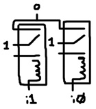
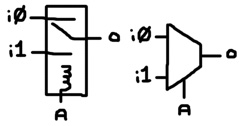
A computational device must be able to direction information from one location in the machine to another. To select data from one of many inputs, a circuit known as a multiplexer (a.k.a. “mux”) is used. Below is a 2-to-1 mux. It provides 2 inputs and 1 output. When A = 0, o = i0. When A = 1, o = i1. The left shows how to construct the circuit with a single relay. The right shows the electronic component symbol for a mux.
Multiple multiplexers can be joined together to form larger ones. Here’s a 4-to-1 mux:
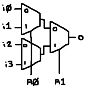
Collectively, the A nodes address the input nodes. For instance, address 10 in binary (A1 = 1 and A0 = 0) is 2 in decimal and input i2 is selected for output.
The following listing shows the construction of an 8-to-1 mux:
# 2-to-1 Mux
def mux a i1 i0 o :
  r a o i1 i0

# 4-to-1 Mux
def mux4to1 a1 a0 i3 i2 i1 i0 o :
  mux a0 i1 i0 x
  mux a0 i3 i2 y
  mux a1 y x o

# 8-to-1 Mux
def mux8to1 a2 a1 a0 i7 i6 i5 i4 i3 i2 i1 i0 o :
  mux4to1 a1 a0 i3 i2 i1 i0 x
  mux4to1 a1 a0 i7 i6 i5 i4 y
  mux a2 y x o
To test the 8-to-1 mux, we’ll set all inputs to 0 except for i4. Then we’ll punch in the address 4 (100 in binary) and verify that the output is 1. Next, we’ll change the address to 5 (101 in binary) and check that the output is 0.
run 100 1 mux8to1   1 0 0   0 0 0 1 0 0 0 0   ?

Build complete: 7 components, 16 nodes.
1: 0
2: 1

run 100 1 mux8to1   1 0 1   0 0 0 1 0 0 0 0   ?

Build complete: 7 components, 15 nodes.
1: 0
Due to the nature of relays, these multiplexers work in reverse. You can treat the output as a single input and the inputs as multiple outputs. That way you can steer a single bit to multiple destinations. Such a circuit is known as a “demultiplexer” or “demux” for short and many books use the same symbol for a mux and a demux.
A demux can be converted into a decoder by permanently setting the input node to 1:
# 3-to-8 Decoder
def decoder3to8 a2 a1 a0 o7 o6 o5 o4 o3 o2 o1 o0 :
  mux8to1 a2 a1 a0 o7 o6 o5 o4 o3 o2 o1 o0 1
A decoder accepts an address and turns on the output that the address refers to. An n-to-m decoder has n address nodes and m output nodes. To test the 3-to-8 decoder above, we’ll address output o4 (100 in binary):
run 100 1 decoder3to8 1 0 0  ? ? ? ? ? ? ? ?

Build complete: 7 components, 16 nodes.
1: 00000001
2: 00010000
In a CPU, many components typically share a common bus. The bus is nothing more a bunch of nodes. The bus is usually drawn as a set of parallel lines, each representing a wire capable of carrying 1 bit of information. All the components that want to communicate are connected to these shared nodes. But, if the components tried to talk over the bus simultaneously, chaos would ensue. Communication between components over the bus must be a controlled process. Essentially, one component will speak to the bus while one or more components listen to the bus.
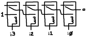
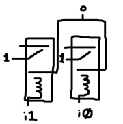
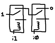
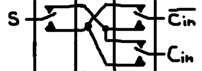
Multi-terminal components connect to the bus via transmission gates:
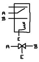
The top of the image shows how to construct a transmission gate with a relay and the bottom shows the electronic component symbol for a transmission gate. A transmission gate allows signals to pass from A to B or from B to A when the enable (E) input is 1. Note that the symbol is an arrow pointing to the right touching an arrow pointing to the left. It almost looks like 2 buffers, but no buffering occurs as the signal passes through the gate.
def trans enabled a b :
  r enabled a b 0

run 10 1 trans 1 1 ?

Build complete: 1 components, 2 nodes.
1: 0
2: 1
Each terminal of a multi-terminal component connects to one of the nodes of the bus through a transmission gate. All the enable input nodes are tied together. Meaning, with the assertion of a single enable signal, a channel between the component and the bus opens. Here’s how to construct such multi-bit transmission gates:
# 2-bit transmission gate
def trans2 enabled a1 a0 b1 b0 :
  trans enabled a1 b1
  trans enabled a0 b0

# 4-bit transmission gate
def trans4 enabled a3 a2 a1 a0 b3 b2 b1 b0 :
  trans2 enabled a3 a2 b3 b2
  trans2 enabled a1 a0 b1 b0

# 8-bit transmission gate
def trans8 enabled a7 a6 a5 a4 a3 a2 a1 a0 b7 b6 b5 b4 b3 b2 b1 b0 :
  trans4 enabled a7 a6 a5 a4 b7 b6 b5 b4
  trans4 enabled a3 a2 a1 a0 b3 b2 b1 b0

# 16-bit transmission gate
def trans16 enabled
    a15 a14 a13 a12 a11 a10 a9 a8 a7 a6 a5 a4 a3 a2 a1 a0
    b15 b14 b13 b12 b11 b10 b9 b8 b7 b6 b5 b4 b3 b2 b1 b0 :
  trans8 enabled a15 a14 a13 a12 a11 a10 a9 a8 b15 b14 b13 b12 b11 b10 b9 b8
  trans8 enabled a7 a6 a5 a4 a3 a2 a1 a0 b7 b6 b5 b4 b3 b2 b1 b0
They can be used for multiplexing. A mux accepts a binary address and directs 1 of several inputs to a single output. Compare that idea to this:
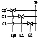
B represents a single node of the bus. C0, C1 and C2 represent terminals from 3 different components that want to share B. You can think of C0, C1 and C2 as inputs and B as a single output. You can select among one of the inputs by asserting the appropriate enable signal. But, the concept goes beyond multiplexing. For instance, C0 and C1 can simultaneously access B by asserting E0 and E1 at the same time. As long as one of those components treats B as an output node and the other treats B as an input node, sharing B works. We’ll return to these idea in a later section.
In the real world, there are many kinds of relays and relay-like devices that retain state. The lever in a latching relay (a.k.a. a keep relay) remains in its last position. Some work similar to those button ballpoint pens where each button press alternately extends or retracts the pen tip. In the relay, an electronic pulse may toggle the position of the lever. That’s achieved though a ratchet mechanism. Another version of the latching relay contains 2 solenoids and the lever is connected to a weak magnet that keeps it stuck to one of the 2 contacts. Momentarily energizing one of the solenoids can overcome the weak magnet and flip the lever to the other state where it remains stuck there.
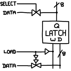
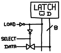
It’s also possible to construct a memory circuit known as a “latch” using the conventional relay discussed thus far. Consider this circuit:
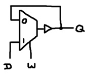
A latch is capable of memorizing 1 bit of information. This latch is constructed out of a 2-to-1 mux and a buffer. It provides 3 terminals: data (D), write (W) and output (Q). Q is the value currently stored in the latch. When W is 0, Q enters the mux, which channeled its value into the buffer. The output of the buffer is Q. The loop keeps Q at some value indefinitely. To set Q to a different value, W is raised to 1. The mux then selects the D input and after a brief delay, the buffer propagates D to Q. When W drops back to 0, the feedback loop is reestablished, effectively memorizing D. Recognize that the loop is not just a loop of wire:
The input of the buffer is the coil of a relay. This achieves 2 important things. First, the loop is constantly refreshed by the power node. Second, since the buffer relay lever may need to toggle, the latch will express the old value for a brief time while accepting a new value. We’ll see how that comes into play a little later. Also, note that it’s okay for D to change while W is 1. As long as D settles on a value before W returns to 0, the latch will remember the final value.
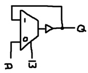
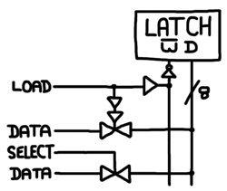
With a slight alteration, the latch can be controlled by write-negative signal:
Let’s define both of these latches:
# Latch, stores when w = 1
def latch w d q :
  mux w d q z
  buf z q

# Latch, stores when w = 0
def latchNeg w d q :
  mux w q d z
  buf z q
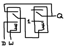
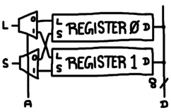
Now, consider what happens if we chain those 2 components together like this:
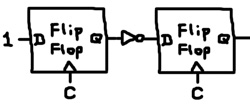
The latch is on the left and the latchNeg is on the right. This creates a 3 terminal electronic component called a “flip flop”. When W is 0, the latch (left) is stuck in its feedback loop and the latchNeg (right) lets the value expressed by the latch (left) to pass through to Q. When W becomes 1, both multiplexers change state, directing the other input terminal to the output. For a brief time (1 iteration), the buffers still reflect the original values. This means that the latchNeg (right) saves the value originally expressed by the latch (left). At the same time, the latch (left) accepts a new value from D. When W drops back to 0, both multiplexers change state again. The latch (left) successfully records D and the latchNeg soon after propagates it out to Q. This means that the flip flop records D when W = 1, but it doesn’t express the new value until W returns to 0. While W = 1, Q is the old value. We’ll utilize this property later when we discuss state machines.
# Flip flop, stores when w rises to 1, expresses new value when w drops to 0
def flipFlop w d q :
  latch w d q2
  latchNeg w q2 q
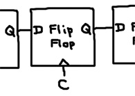
Latches and flip flops store single bits of information. To store a few bytes of information, they can be grouped together to form registers. For example, here is a 1-byte register made of flip flops:
def flipFlopRegister w d7 d6 d5 d4 d3 d2 d1 d0 q7 q6 q5 q4 q3 q2 q1 q0:
  flipFlop w d7 q7
  flipFlop w d6 q6
  flipFlop w d5 q5
  flipFlop w d4 q4
  flipFlop w d3 q3
  flipFlop w d2 q2
  flipFlop w d1 q1
  flipFlop w d0 q0
Flip flop registers are the easiest type to work with. In a computing device, the input and output terminals are connected to multiple places via transmissions gates.
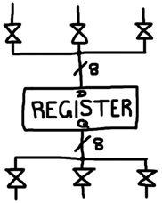
The slash-8 indicates that the line actually represents a set of 8 wires, which also implies that those are 8-bit transmission gates. The control lines that open and close the transmission gates are not shown. The control signals would normally originate from a state machine, a topic discussed below.
To “load” the register with a new value, one of the transmission gates connected to the register’s input terminals would be opened and the write signal would be asserted. To “select” the value stored in a register and direct it to somewhere else in the machine, one of the transmission gates connected to the register’s output terminals would be opened.
In the case of a flip flop register, the write signal is usually connected to the clock. When the clock is 1, a state machine would open the appropriate transmission gate and let a value flow into the register. When the clock drops to 0, the new value is saved and expressed to the output terminals. For example, you can connect the outputs of 3 registers to the inputs of an adder via transmission gates. And you can connect the output of the adder to the inputs of the registers again via transmission gates.
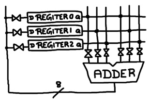
With this configuration, it’s possible to select any register as an input to the adder and load the sum into any register. In fact, since a flip flop doesn’t express a new value until its write signal drops to 0, you can select a register for the adder and load the sum back into the very same register. Or even double the value in a register by selecting the same register twice for the adder.
The adder may take a few simulation iterations to settle on the correct sum. During that time, the register being loaded will receive a changing value. Recall that it doesn’t matter if the input value of a flip flop is changing when the write signal is 1. It captures a new value at the moment that the write signal drops to 0. The clock cycle must be adjusted appropriately to ensure that the write signal drops after all input values have settled. If the clock cycle is too fast, the register may load the wrong the value.
With the write signal connected to the clock, a flip flop register gains a new value once per clock cycle. For a particular clock cycle, if the state machine fails to open any transmission gate connected to the register’s input terminals, the register will get erased (i.e. it will be cleared to all 0’s). A simple solution is to connect the output of the flip flop back to the input via a transmission gate. When the register doesn’t need to load a value from somewhere else, the state machine will open that transmission gate enabling the register to load itself.
An alternative to a flip flop register is a latch register:
def latchRegister w d7 d6 d5 d4 d3 d2 d1 d0 q7 q6 q5 q4 q3 q2 q1 q0:
  latch w d7 q7
  latch w d6 q6
  latch w d5 q5
  latch w d4 q4
  latch w d3 q3
  latch w d2 q2
  latch w d1 q1
  latch w d0 q0
To load the register, a state machine would assert a signal that simultaneously sets write to 1 and opens a transmission gate. When the load signal drops, it’s important that write signal becomes 0 slightly sooner than the transmission gate closes or else the latch may end up saving the wrong value. You can achieve that with a few buffers:
The load signal is separated from the write line via a buffer. That buffer allows multiple load signals to share the same write line, collectively forming a multi-input OR gate. The load signal is connect to the enable input of a transmission gate via 2 buffers. Changes to the load signal propagate to the write line faster than to the transmission gate. When the load signal drops, the transmission gate will remain open long enough for the latch to store the correct value.
Selecting the output is the same as before; however, due to the nature of a latch, it is not possible to select and load from the same register.
It’s actually possible to construct a type of latch out of a single relay:
The write signal is negatively asserted. To store a value, it drops from 1 to 0. That enables D to change the position of the relay lever since it is connected to the relay coil. When the write terminal rises back to 1, if the lever is touching the normally-disconnected terminal, that 1 value will travel through the lever and to the coil, keeping the lever in that position. If the lever were touching the other terminal, that pathway won’t exist and lever remains in the relaxed state.
Unlike the latch presented above, this latch doesn’t have an output terminal. The data terminal acts as both input and output. To construct a register, we’ll tie the negative-write terminals of 8 of these latches together:
def tinyLatchRegister writeNeg d7 d6 d5 d4 d3 d2 d1 d0 :
  r d7 d7 writeNeg 0
  r d6 d6 writeNeg 0
  r d5 d5 writeNeg 0
  r d4 d4 writeNeg 0
  r d3 d3 writeNeg 0
  r d2 d2 writeNeg 0
  r d1 d1 writeNeg 0
  r d0 d0 writeNeg 0
Loading a value onto this latch register involves similar circuitry as the previous latch register:
The write line is connected to the negative-write terminal of the latch via an inverter and the load signal is separated from the write line by a buffer to allow multiple load signals to share the line. If there were multiple load signals, the buffers and the inverter would collectively form a multi-input NOR gate feeding the negative-write terminal. The load signal also opens a transmission gate and the double buffer ensures that the transmission gate remains open long enough to store a value when the load signal drops.
This is a very temperamental type of latch. Note that a pathway occasionally exists between the data terminal and the negative-write terminal. When loading a value into the register, if a single bit of the value is a 1, then not only will a pathway form between the data terminal and the negative-write terminal of one of the latches, but the negative-write terminal will now have logic 1. Since all the negative-write terminals are tied together in the register, it’s effectively the same as the negative-write signal of the register rising to 1. But, it should be 0 when you are trying to load a value. This means that as soon as the 8-bit transmission gate that feeds the data terminals of the register opens, the latch will trap the new value instantly. Unlike the flip flop and the previous latch, you can’t feed this latch a changing, unsettled input value.
In a CPU, registers serve as tiny amounts of fast computer memory storing some of the variable values of a program being executed. But, a computer also needs access to large amounts of RAM to store the program itself and its associated data. It’s not very practical to build the main memory of a computer out of relays because of the enormous number of relays involved. But, if you were to build it, you might as use the aforementioned, temperamental latch register because it only uses 1 relay per bit of information.
Our main memory will consist of hundreds or thousands of latch registers. You’ll need to provide an address to direction information to or from a particular latch. All of the latches will share a common data bus. As a step in that direction, we’ll construct this circuit:
def memoryRegister select load d7 d6 d5 d4 d3 d2 d1 d0 :
  inv load writeNeg
  inv writeNeg select
  trans8 select d7 d6 d5 d4 d3 d2 d1 d0 z7 z6 z5 z4 z3 z2 z1 z0
  tinyLatchRegister writeNeg z7 z6 z5 z4 z3 z2 z1 z0
We can address 2 of these registers using demultiplexers:
# 2 Bytes of memory
def memory2 address select load d7 d6 d5 d4 d3 d2 d1 d0 :
  mux address select1 select0 select
  mux address load1 load0 load
  memoryRegister select0 load0 d7 d6 d5 d4 d3 d2 d1 d0
  memoryRegister select1 load1 d7 d6 d5 d4 d3 d2 d1 d0
The value of the address terminal determines which of the 2 registers has access to the load and select signals. Also, note that the mux component is being used as a demultiplexer here. This can be doubled-up indefinitely:
# 4 Bytes of memory
def memory4 a1 a0 select load d7 d6 d5 d4 d3 d2 d1 d0 :
  mux a1 select1 select0 select
  mux a1 load1 load0 load
  memory2 a0 select load d7 d6 d5 d4 d3 d2 d1 d0
  memory2 a0 select load d7 d6 d5 d4 d3 d2 d1 d0

# 8 Bytes of memory
def memory8 a2 a1 a0 select load d7 d6 d5 d4 d3 d2 d1 d0 :
  mux a2 select1 select0 select
  mux a2 load1 load0 load
  memory4 a1 a0 select load d7 d6 d5 d4 d3 d2 d1 d0
  memory4 a1 a0 select load d7 d6 d5 d4 d3 d2 d1 d0

# 16 Bytes of memory
def memory16 a3 a2 a1 a0 select load d7 d6 d5 d4 d3 d2 d1 d0 :
  mux a3 select1 select0 select
  mux a3 load1 load0 load
  memory8 a2 a1 a0 select load d7 d6 d5 d4 d3 d2 d1 d0
  memory8 a2 a1 a0 select load d7 d6 d5 d4 d3 d2 d1 d0

# 32 Bytes of memory
def memory32 a4 a3 a2 a1 a0 select load d7 d6 d5 d4 d3 d2 d1 d0 :
  mux a4 select1 select0 select
  mux a4 load1 load0 load
  memory16 a3 a2 a1 a0 select load d7 d6 d5 d4 d3 d2 d1 d0
  memory16 a3 a2 a1 a0 select load d7 d6 d5 d4 d3 d2 d1 d0

# 64 Bytes of memory
def memory64 a5 a4 a3 a2 a1 a0 select load d7 d6 d5 d4 d3 d2 d1 d0 :
  mux a5 select1 select0 select
  mux a5 load1 load0 load
  memory32 a4 a3 a2 a1 a0 select load d7 d6 d5 d4 d3 d2 d1 d0
  memory32 a4 a3 a2 a1 a0 select load d7 d6 d5 d4 d3 d2 d1 d0

# 128 Bytes of memory
def memory128 a6 a5 a4 a3 a2 a1 a0 select load d7 d6 d5 d4 d3 d2 d1 d0 :
  mux a6 select1 select0 select
  mux a6 load1 load0 load
  memory64 a5 a4 a3 a2 a1 a0 select load d7 d6 d5 d4 d3 d2 d1 d0
  memory64 a5 a4 a3 a2 a1 a0 select load d7 d6 d5 d4 d3 d2 d1 d0

# 256 Bytes of memory
def memory256 a7 a6 a5 a4 a3 a2 a1 a0 select load d7 d6 d5 d4 d3 d2 d1 d0 :
  mux a7 select1 select0 select
  mux a7 load1 load0 load
  memory128 a6 a5 a4 a3 a2 a1 a0 select load d7 d6 d5 d4 d3 d2 d1 d0
  memory128 a6 a5 a4 a3 a2 a1 a0 select load d7 d6 d5 d4 d3 d2 d1 d0
We'll stop at 256 bytes and check how many relays we consumed in the process by reading from address 0:
run 100 1 memory256 0 0 0 0 0 0 0 0  1 0  ? ? ? ? ? ? ? ?

Build complete: 5118 components, 7949 nodes.
1: 00000000
That’s already many times the number of relays required for a simple CPU.
Now for a reality check. The original latch described above consists of a mux and a buffer.
When the write signal (W) drops from 1 to 0, a feedback loop forms and the latch consequentially stores a value. But, the mux is built with a single relay where W connects to the coil of that relay. When W drops from 1 to 0, the lever in that relay physically jumps between terminals. During that brief swinging time, the lever is essentially a floating wire. No power can possibly be reaching the buffer during that time. Will the buffer relay lever as a consequence return to the relaxed state regardless of the value D?
The magnetic field of a solenoid doesn’t dissipate immediately at the moment that power is cutoff. The intensity of the field will start to drop as soon as power is removed, but as long as it doesn’t drop below a certain threshold before power is restored, the position of the lever will remain the same. You can slow the process down further using a capacitor like this:
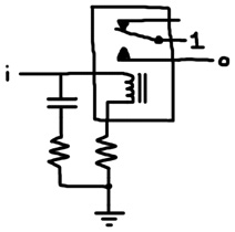
When power is supplied to node i, the relay lever toggles as before and the capacitor rapidly charges to the power voltage. When power is cutoff, the capacitor temporarily acts like a battery as it discharges through the loop consisting of the relay coil and the resistors. You can prevent the relay from returning to the relaxed position for any desired duration by selecting the proper capacitance and resistance values; however, since the buffer reacts slower to changes in input, you’ll need to use a longer clock period to compensate. Also, since the capacitor acts like a battery, it’s possible for it to discharge backwards through the mux relay and out of the D input of the flip flop. Luckily, if you are only working in the simulated world of Tofu, you don’t need to be concerned about any of this. There is no brief relay lever swinging time in the simulation. The levers flip instantly.
Check out this circuit:
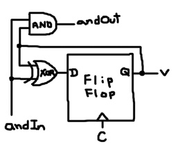
The clock is tied to the write node of the flip flop; so, every time the clock moves from 1 to 0, a new value might be expressed. Suppose andIn is 1. Anything XORed against 1 is inverted. Since the output of the flip flop, V, is fed back into the flip flop through the XOR gate, V toggles every clock cycle. This is a counting element. We’ll assemble many of them together and each V will represent one binary digit in the value of counter. The andIn signal will be 1 only when all the lower digits are all 1. If they’re all 1, then it’s time for this digit to change. andIn ANDed with V produces andOut, which is used as the andIn signal of the next counting element. The initial andIn is set to 1; meaning, the lowest digit should always be toggling.
def counterElement andIn andOut value :
  xor andIn value data
  flipFlop c data value
  and andIn value andOut
One key thing to note here is that the output of the flip flop along with other data (in this case the lower digits) is used to generate a new value of the flip flop. This is not possible with a latch because the output of a latch changes when the write signal is 1. A flip flop continues to express the old value while storing a new value. Now, let’s create an 8-bit counter and test it out:
def counter2 andIn andOut v1 v0 :
  counterElement andIn x v0
  counterElement x andOut v1

def counter4 andIn andOut v3 v2 v1 v0 :
  counter2 andIn x v1 v0
  counter2 x andOut v3 v2

def counter8 andIn andOut v7 v6 v5 v4 v3 v2 v1 v0 :
  counter4 andIn x v3 v2 v1 v0
  counter4 x andOut v7 v6 v5 v4

run 160 5 counter8 1 0 ? ? ? ? ? ? ? ?

Build complete: 64 components, 104 nodes.
1: 00000000
7: 00000001
17: 00000010
27: 00000011
37: 00000100
47: 00000101
57: 00000110
67: 00000111
77: 00001000
87: 00001001
97: 00001010
107: 00001011
117: 00001100
127: 00001101
137: 00001110
147: 00001111
157: 00010000
Notice the count changes every 10 iterations because we specified 5 for the half clock period.
A counter is a simple example of a state machine. The realization of state machines that are discussed here consist of memory in the form of flip flops and logic that determines what the next state should be. The next state is recorded by the flip flops and cycle continues. In a CPU, a state machine controls the signal inputs (e.g. load and select) of the components, enabling data to move around as an organized process. The states that the state machine in a CPU goes through are governed by the instructions in memory.
Now, let’s create an 8-bit shift register:
def shift2 shiftIn q1 q0 :
  flipFlop c shiftIn q1
  flipFlop c q1 q0

def shift4 shiftIn q3 q2 q1 q0 :
  shift2 shiftIn q3 q2
  shift2 q2 q1 q0

def shift8 shiftIn q7 q6 q5 q4 q3 q2 q1 q0 :
  shift4 shiftIn q7 q6 q5 q4
  shift4 q4 q3 q2 q1 q0
The shift register consists of 8 flip flops chained together such that the output of one flip flop is connected to the data node of the next flip flop in the chain.
All the write signals are tied to the clock node. When the clock becomes 1, each flip flop records the value expressed by the flip flop to the left while continuing to express the old value. When the clock becomes 0, the flip flops express the new values and the value in the register has consequentially been shifted to the right. The shiftIn node allows you to specify what value fills in the left-most bit during shifting. Let’s set that to 1 and see what happens:
run 100 5 shift8 1 ? ? ? ? ? ? ? ?

Build complete: 32 components, 48 nodes.
1: 00000000
7: 10000000
17: 11000000
27: 11100000
37: 11110000
47: 11111000
57: 11111100
67: 11111110
77: 11111111
Instead of feeding 1 into shiftIn, consider adding an extra flip flop and an inverter like this:
def shiftOne q7 q6 q5 q4 q3 q2 q1 q0 :
  flipFlop c 1 q
  inv q shiftIn
  shift8 shiftIn q7 q6 q5 q4 q3 q2 q1 q0
The extra flip flop initially outputs 0, but after the first clock cycle, it indefinitely outputs 1. That output is inverted before it reaches the shiftIn terminal. Hence, the shift register pulls in a 1 followed by all 0’s:
run 100 5 shiftOne ? ? ? ? ? ? ? ?

Build complete: 37 components, 56 nodes.
1: 00000000
7: 10000000
17: 01000000
27: 00100000
37: 00010000
47: 00001000
57: 00000100
67: 00000010
77: 00000001
87: 00000000
We can successively connect the shift-out terminal to a buffer and feed it back into shiftIn:
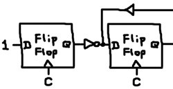
def loop q7 q6 q5 q4 q3 q2 q1 q0 :
  flipFlop c 1 q
  inv q shiftIn
  shift8 shiftIn q7 q6 q5 q4 q3 q2 q1 q0
  buf q0 shiftIn

run 200 5 loop ? ? ? ? ? ? ? ?

Build complete: 38 components, 57 nodes.
1: 00000000
7: 10000000
17: 01000000
27: 00100000
37: 00010000
47: 00001000
57: 00000100
67: 00000010
77: 00000001
87: 10000000
97: 01000000
107: 00100000
117: 00010000
127: 00001000
137: 00000100
147: 00000010
157: 00000001
167: 10000000
177: 01000000
187: 00100000
197: 00010000
If this were reduced to a 3-bit register, it could control a traffic light: green, yellow, red, green, yellow, red, etc. A traffic light is a simple state machine with 3 states. Each state is associated with a separate bulb. The 8-bit shift register can be considered a state machine with 8 states, each associated with the output of a separate flip flop. That extra flip flop boots up our little machine by getting it into the first state. The machine goes from one state to the next and then back to the first. It’s stuck in an infinite loop.
In this section, we’ll apply many of the ideas discussed above to construct a simple computing device capable of multiplying 2 numbers together. Multiplication in binary can be performed by the same technique people learn to do it in decimal on paper. When you multiply multi-digit numbers, you actually multiply the first value against each digit of the second value. That produces a series of products which are added up; however, each product must be shifted over to the left to align it with digit used to multiply before adding. The answer is the sum of all the shifted products.
Multiplying the first value against a digit of the second value in binary is very easy. If the digit is 0, then the product is 0. If the digit is 1, then the product is the original value. Let’s multiply two 4-bit numbers to see this in action:
    0011
  x 0101
    ----
    0011
   0000
  0011
 0000
--------
00001111
Above we multiply 3 and 5 to produce 15. This was accomplished by multiplying the first value (0011) against each digit of the second value (0101). Each product is shifted to the left to align it with the digit we multiplied with. The space to the right of the shifted value is filled in with 0’s, which are not shown for clarity. The shifted values are added up to produce the answer, which may require up to 8-bits (in general the product of two n-bit numbers is a 2n-bit number).
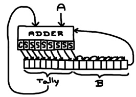
This technique suggests a very simple circuit. Consider multiplying two 8-bit numbers. That means we’ll produce 8 products that need to be shifted and added up. We can tally 8 numbers by hooking together 8 multi-bit adders. That will use an excessive number of relays, but it will work. We’ll use 16-bit adders and we’ll accomplish the shifting by wiring the first 8-bit number to different shifted positions on each adder. So, each adder will accept a shifted number and a partial tally. But, we only want to add if the associated digit in the second number is a 1; otherwise, we want to leave the tally as it is. We’ll start out by building an adder with that property:
# 1-bit adder
def mAdder add carryInNeg carryIn a b carryOutNeg carryOut sum :
  trans add b s
  zuseFullAdder carryInNeg carryIn a s carryOutNeg carryOut sum
mAdder is built around the zuseFullAdder discussed above. The only difference is an extra input called “add”. When add is 1, it sums a and b. When add is 0, it sums a and 0. This is accomplished by connecting b to the zuseFullAdder through a transmission gate that is controlled by the add input. Here, a represents a digit of the tally and b represents a digit of the shifted number. The add input is actually a digit of the second number to be multiplied. Let’s double-up this up to 16-bits:
# 2-bit adder
def mAdder2 add carryInNeg carryIn a1 a0 b1 b0 carryOutNeg carryOut s1 s0 :
  mAdder add carryInNeg carryIn a0 b0 cOutNeg cOut s0
  mAdder add cOutNeg cOut a1 b1 carryOutNeg carryOut s1

# 4-bit adder
def mAdder4 add carryInNeg carryIn a3 a2 a1 a0 b3 b2 b1 b0
    carryOutNeg carryOut s3 s2 s1 s0 :
  mAdder2 add carryInNeg carryIn a1 a0 b1 b0 cOutNeg cOut s1 s0
  mAdder2 add cOutNeg cOut a3 a2 b3 b2 carryOutNeg carryOut s3 s2

# 8-bit adder
def mAdder8 add
    carryInNeg carryIn   a7 a6 a5 a4 a3 a2 a1 a0
                         b7 b6 b5 b4 b3 b2 b1 b0
    carryOutNeg carryOut s7 s6 s5 s4 s3 s2 s1 s0 :
  mAdder4 add carryInNeg carryIn a3 a2 a1 a0 b3 b2 b1 b0
      cOutNeg cOut s3 s2 s1 s0
  mAdder4 add cOutNeg cOut a7 a6 a5 a4 b7 b6 b5 b4
      carryOutNeg carryOut s7 s6 s5 s4

# 16-bit adder
def mAdder16 add
    carryInNeg carryIn   a15 a14 a13 a12 a11 a10 a9 a8 a7 a6 a5 a4 a3 a2 a1 a0
                         b15 b14 b13 b12 b11 b10 b9 b8 b7 b6 b5 b4 b3 b2 b1 b0
    carryOutNeg carryOut s15 s14 s13 s12 s11 s10 s9 s8 s7 s6 s5 s4 s3 s2 s1 s0 :
  mAdder8 add carryInNeg carryIn a7 a6 a5 a4 a3 a2 a1 a0 b7 b6 b5 b4 b3 b2 b1 b0
      cOutNeg cOut s7 s6 s5 s4 s3 s2 s1 s0
  mAdder8 add cOutNeg cOut
      a15 a14 a13 a12 a11 a10 a9 a8 b15 b14 b13 b12 b11 b10 b9 b8
      carryOutNeg carryOut s15 s14 s13 s12 s11 s10 s9 s8
To make a multiplier, we need to hook up 8 of them like this:
def multiplier
    a7 a6 a5 a4 a3 a2 a1 a0
    b7 b6 b5 b4 b3 b2 b1 b0
    p15 p14 p13 p12 p11 p10 p9 p8 p7 p6 p5 p4 p3 p2 p1 p0 :
  mAdder16 b0 1 0
      0 0 0 0 0 0 0 0 0 0 0 0 0 0 0 0
      0 0 0 0 0 0 0 0 a7 a6 a5 a4 a3 a2 a1 a0
      0 0 d15 d14 d13 d12 d11 d10 d9 d8 d7 d6 d5 d4 d3 d2 d1 d0
  mAdder16 b1 1 0
      d15 d14 d13 d12 d11 d10 d9 d8 d7 d6 d5 d4 d3 d2 d1 d0
      0 0 0 0 0 0 0 a7 a6 a5 a4 a3 a2 a1 a0 0
      0 0 e15 e14 e13 e12 e11 e10 e9 e8 e7 e6 e5 e4 e3 e2 e1 e0
  mAdder16 b2 1 0
      e15 e14 e13 e12 e11 e10 e9 e8 e7 e6 e5 e4 e3 e2 e1 e0
      0 0 0 0 0 0 a7 a6 a5 a4 a3 a2 a1 a0 0 0
      0 0 f15 f14 f13 f12 f11 f10 f9 f8 f7 f6 f5 f4 f3 f2 f1 f0
  mAdder16 b3 1 0
      f15 f14 f13 f12 f11 f10 f9 f8 f7 f6 f5 f4 f3 f2 f1 f0
      0 0 0 0 0 a7 a6 a5 a4 a3 a2 a1 a0 0 0 0
      0 0 g15 g14 g13 g12 g11 g10 g9 g8 g7 g6 g5 g4 g3 g2 g1 g0
  mAdder16 b4 1 0
      g15 g14 g13 g12 g11 g10 g9 g8 g7 g6 g5 g4 g3 g2 g1 g0
      0 0 0 0 a7 a6 a5 a4 a3 a2 a1 a0 0 0 0 0
      0 0 h15 h14 h13 h12 h11 h10 h9 h8 h7 h6 h5 h4 h3 h2 h1 h0
  mAdder16 b5 1 0
      h15 h14 h13 h12 h11 h10 h9 h8 h7 h6 h5 h4 h3 h2 h1 h0
      0 0 0 a7 a6 a5 a4 a3 a2 a1 a0 0 0 0 0 0
      0 0 i15 i14 i13 i12 i11 i10 i9 i8 i7 i6 i5 i4 i3 i2 i1 i0
  mAdder16 b6 1 0
      i15 i14 i13 i12 i11 i10 i9 i8 i7 i6 i5 i4 i3 i2 i1 i0
      0 0 a7 a6 a5 a4 a3 a2 a1 a0 0 0 0 0 0 0
      0 0 j15 j14 j13 j12 j11 j10 j9 j8 j7 j6 j5 j4 j3 j2 j1 j0
  mAdder16 b7 1 0
      j15 j14 j13 j12 j11 j10 j9 j8 j7 j6 j5 j4 j3 j2 j1 j0
      0 a7 a6 a5 a4 a3 a2 a1 a0 0 0 0 0 0 0 0
      0 0 p15 p14 p13 p12 p11 p10 p9 p8 p7 p6 p5 p4 p3 p2 p1 p0
The first mAdder16 starts out with a tally of 0 and adds A. The second mAdder16 takes the partial tally from the first mAdder16 and adds A shifted 1 digit to the left. The third mAdder16 takes the partial tally from the second mAdder16 and adds A shifted 2 digits to the left, and so on. Note that the add input of each mAdder16 is a separate digit of B, controlling when to add the shifted A and when to leave the tally alone (it adds 0 instead of the shifted A).
Now, let’s test it out. Let’s multiply 100 (01100100) and 200 (11001000) to produce the product 20,000 (0100111000100000):
# 100 x 200 = 20,000
run 100 1 multiplier
    0 1 1 0 0 1 0 0
    1 1 0 0 1 0 0 0
    ? ? ? ? ? ? ? ? ? ? ? ? ? ? ? ?

Build complete: 1152 components, 1506 nodes.
1: 0000000000000000
3: 0011001000000000
4: 0100101100000000
7: 0100111000100000
It consumed a lot of relays, but at least it’s really fast.
What about signed numbers? When people multiply multi-digit numbers on paper, they initially ignore the signs and compute the product of 2 positive numbers. Then the 2 signs are taken into account to give the product the appropriate sign. We can apply that technique here as well. We can use the sign bit (the left-most bit) of each number to determine if we need to negate the number, perform the multiplication with positive numbers and use the sign bits again to determine if we need to negate the product. To negate a value, we can use our adderSubtractor. For a some value A, we’ll compute 0 – A when A is negative and we’ll compute 0 + A when A is positive. The adderSubtractor defined above was designed for 8-bit numbers. We’ll need a 16-bit version:
# 16-bit Partial Adder/Subtractor
def xFullAdder16 subtract carryInNeg carryIn
                         a15 a14 a13 a12 a11 a10 a9 a8 a7 a6 a5 a4 a3 a2 a1 a0
                         b15 b14 b13 b12 b11 b10 b9 b8 b7 b6 b5 b4 b3 b2 b1 b0
    carryOutNeg carryOut s15 s14 s13 s12 s11 s10 s9 s8 s7 s6 s5 s4 s3 s2 s1 s0 :
  xFullAdder8 subtract carryInNeg carryIn
      a7 a6 a5 a4 a3 a2 a1 a0 b7 b6 b5 b4 b3 b2 b1 b0
      cOutNeg cOut s7 s6 s5 s4 s3 s2 s1 s0
  xFullAdder8 subtract cOutNeg cOut
      a15 a14 a13 a12 a11 a10 a9 a8 b15 b14 b13 b12 b11 b10 b9 b8
      carryOutNeg carryOut s15 s14 s13 s12 s11 s10 s9 s8

# 16-bit Adder/Subtractor
def adderSubtractor16 subtract
             a15 a14 a13 a12 a11 a10 a9 a8 a7 a6 a5 a4 a3 a2 a1 a0
             b15 b14 b13 b12 b11 b10 b9 b8 b7 b6 b5 b4 b3 b2 b1 b0
    carryOut s15 s14 s13 s12 s11 s10 s9 s8 s7 s6 s5 s4 s3 s2 s1 s0 :
  inv subtract carryInNeg
  xFullAdder16 subtract carryInNeg subtract
                       a15 a14 a13 a12 a11 a10 a9 a8 a7 a6 a5 a4 a3 a2 a1 a0
                       b15 b14 b13 b12 b11 b10 b9 b8 b7 b6 b5 b4 b3 b2 b1 b0
      carryOutNeg cOut s15 s14 s13 s12 s11 s10 s9 s8 s7 s6 s5 s4 s3 s2 s1 s0
  xor cOut subtract carryOut
We’ll use it to wrap the multiplier to provide signed multiplication:
def signedMultiplier signed
    a7 a6 a5 a4 a3 a2 a1 a0
    b7 b6 b5 b4 b3 b2 b1 b0
    p15 p14 p13 p12 p11 p10 p9 p8 p7 p6 p5 p4 p3 p2 p1 p0 :
  and signed a7 negateA
  and signed b7 negateB
  adderSubtractor negateA 0 0 0 0 0 0 0 0
      a7 a6 a5 a4 a3 a2 a1 a0 0 c7 c6 c5 c4 c3 c2 c1 c0
  adderSubtractor negateB 0 0 0 0 0 0 0 0
      b7 b6 b5 b4 b3 b2 b1 b0 0 d7 d6 d5 d4 d3 d2 d1 d0
  multiplier
      c7 c6 c5 c4 c3 c2 c1 c0
      d7 d6 d5 d4 d3 d2 d1 d0
      q15 q14 q13 q12 q11 q10 q9 q8 q7 q6 q5 q4 q3 q2 q1 q0
  xor a7 b7 negateProduct
  and signed negateProduct negateQ
  adderSubtractor16 negateQ 0 0 0 0 0 0 0 0 0 0 0 0 0 0 0 0
      q15 q14 q13 q12 q11 q10 q9 q8 q7 q6 q5 q4 q3 q2 q1 q0
      0 p15 p14 p13 p12 p11 p10 p9 p8 p7 p6 p5 p4 p3 p2 p1 p0
Note the extra signed input. When signed is 1, it treats A and B as signed numbers. The adderSubtractors negate A and B when signed is 1 and their sign bits are 1. The values are fed into the multiplier, which produces the product Q. Q is negated when signed is 1 and the sign bits of A and B don’t match. That check is done with an XOR gate. Now, let’s run a few tests:
# 3 x 5 = 15
run 100 1 signedMultiplier 1
    0 0 0 0 0 0 1 1
    0 0 0 0 0 1 0 1
    ? ? ? ? ? ? ? ? ? ? ? ? ? ? ? ?

Build complete: 1489 components, 1954 nodes.
1: 0000000000000000
12: 0000000000001100
14: 0000000000001111

# -3 x 5 = -15
run 100 1 signedMultiplier 1
    1 1 1 1 1 1 0 1
    0 0 0 0 0 1 0 1
    ? ? ? ? ? ? ? ? ? ? ? ? ? ? ? ?

Build complete: 1489 components, 1949 nodes.
1: 0000000000000000
3: 0000000000000001
5: 0000000000000000
12: 1111111111110100
14: 1111111111110001

# 3 x -5 = -15
run 100 1 signedMultiplier 1
    0 0 0 0 0 0 1 1
    1 1 1 1 1 0 1 1
    ? ? ? ? ? ? ? ? ? ? ? ? ? ? ? ?

Build complete: 1489 components, 1949 nodes.
1: 0000000000000000
3: 0000000000000001
5: 0000000000000000
7: 1111111010000000
8: 1111111101000000
9: 1111111110100000
10: 1111111111010000
11: 1111111111101000
12: 1111111111110100
13: 1111111111110001
14: 1111111111110100
15: 1111111111110001

# -3 x -5 = 15
run 100 1 signedMultiplier 1
    1 1 1 1 1 1 0 1
    1 1 1 1 1 0 1 1
    ? ? ? ? ? ? ? ? ? ? ? ? ? ? ? ?

Build complete: 1489 components, 1944 nodes.
1: 0000000000000000
7: 0000000110000000
8: 0000000011000000
9: 0000000001100000
10: 0000000000110000
11: 0000000000011000
12: 0000000000001100
13: 0000000100001010
14: 0000000000001100
15: 0000000000001111

# 255 x 255 = 65025
run 100 1 signedMultiplier 0
    1 1 1 1 1 1 1 1
    1 1 1 1 1 1 1 1
    ? ? ? ? ? ? ? ? ? ? ? ? ? ? ? ?

Build complete: 1489 components, 1943 nodes.
1: 0000000000000000
7: 0111111110000000
8: 1011111101000000
9: 1101111100100000
10: 1110111100010000
11: 1111011100001000
12: 1111101100000100
13: 1111110100000010
14: 1111111000000001

# -1 x -1 = 1
run 100 1 signedMultiplier 1
    1 1 1 1 1 1 1 1
    1 1 1 1 1 1 1 1
    ? ? ? ? ? ? ? ? ? ? ? ? ? ? ? ?

Build complete: 1489 components, 1942 nodes.
1: 0000000000000000
15: 0000000000000001
We can build a multiplier with fewer relays by reusing the same adder for all the additions. A state machine will govern the 8 additions and shifts necessary to multiply two 8-bit values. We’ll start out by constructing an 8-input OR gate that’ll come in handy later:
# 4-input OR gate
def or4 i3 i2 i1 i0 o :
  or i3 i2 o
  or i1 i0 o

# 8-input OR gate
def or8 i7 i6 i5 i4 i3 i2 i1 i0 o :
  or4 i7 i6 i5 i4 o
  or4 i3 i2 i1 i0 o
It’s effectively equivalent to 8 buffers in parallel.
When you multiply 2 binary numbers by hand, as shown in the example above, you multiple the first number against each digit of the second number and you write down those products such that they align with the digit you multiplied by. At the end, you add them all up.
    0011
  x 0101
    ----
    0011
   0000
  0011
 0000
--------
00001111
An alternative way is to keep a running tally. Meaning, after the single digit multiplication, add the product to the running tally then shift to keep things aligned:
1 x 0011 = 0011
         + 0000
         ------
          00011

0 x 0011 = 0000
         + 00011
           -----
          000011

1 x 0011 = 0011
         + 000011
           ------
          0001111

0 x 0011 = 0000
         + 0001111
           -------
          00001111
Each addition actually produces 1 digit of the final answer (the right-most digit). After the addition that digit won’t be touched. This means that to multiple two n-bit numbers, we only need an n-bit adder as opposed to a 2n-bit adder. Also, note that each addition produces a carry (in this case all the carry bits were zero). We need to include that when we shift.
To multiply two 8-bit numbers, A and B, we’ll use a 16-bit register constructed out of 16 flip flops. First, we’ll copy B onto the lower 8-bits of the register. The upper 8-bits will contain the running tally, which starts out as 0. We need to multiply A times each bit of B, adding to our tally and shifting as we go. Each time the register is right-shifted, a bit of B disappears and the right-most bit of the register contains the next bit of B. So, we’ll use the right-most bit of the register to control the adder. When the right-most bit is 1, we’ll add A to the tally. When the right-most bit is 0, we’ll leave the tally as it is.
We’ll construct the multiplier definition in pieces. First, the 16-bit register:
def multiplier2
    a7 a6 a5 a4 a3 a2 a1 a0
    b7 b6 b5 b4 b3 b2 b1 b0
    p15 p14 p13 p12 p11 p10 p9 p8 p7 p6 p5 p4 p3 p2 p1 p0 :

  # 16-bit register made of flip flops
  flipFlop c d15 p15
  flipFlop c d14 p14
  flipFlop c d13 p13
  flipFlop c d12 p12
  flipFlop c d11 p11
  flipFlop c d10 p10
  flipFlop c d9 p9
  flipFlop c d8 p8
  flipFlop c d7 p7
  flipFlop c d6 p6
  flipFlop c d5 p5
  flipFlop c d4 p4
  flipFlop c d3 p3
  flipFlop c d2 p2
  flipFlop c d1 p1
  flipFlop c d0 p0
The register is updated each time the clock drops from 1 to 0. So, for each clock cycle, if we fail to expose the data input bits to some value, the register will erase itself (all bits will become 0). We’ll expose the data input bits to different values using transmission gates. The enable signals for the transmission gates will be governed by a state machine.
To get B into the lower 8 bits of the register, we’ll use an 8-bit transmission gate. We define a signal called loadB. When loadB is 1, B is exposed to the lower 8 data input bits of the register. Since the transmission gate won’t touch the upper 8 bits of the register, when the clock drops from 1 to 0, those bits will become zero.
trans8 loadB d7 d6 d5 d4 d3 d2 d1 d0 b7 b6 b5 b4 b3 b2 b1 b0
The right-most bit of the register, p0, acts a signal to control an 8-bit adder. When p0 is 1, the adder adds A to the upper 8-bits of the register (the running tally). When p0 is 0, the adder adds 0 to the upper 8-bits of the register. We’ll do this with another 8-bit transmission gate:
  trans8 p0 a7 a6 a5 a4 a3 a2 a1 a0 z7 z6 z5 z4 z3 z2 z1 z0
  zuseAdder8 1 0 p15 p14 p13 p12 p11 p10 p9 p8 z7 z6 z5 z4 z3 z2 z1 z0
      0 s8 s7 s6 s5 s4 s3 s2 s1 s0
Note that s8 is the carry bit. Now, what to do with that sum? It needs to be exposed to the data input bits of the register and we need to shift the register. Both can be accomplished with a 16-bit transmission gate. We define a signal called tallyShift that will replace the upper 9 bits of the register with the carry and the 8 sum bits and shift the remaining bits to the right. The right-most bit will disappear.
  trans16 tallyShift d15 d14 d13 d12 d11 d10 d9 d8 d7 d6 d5 d4 d3 d2 d1 d0
      s8 s7 s6 s5 s4 s3 s2 s1 s0 p7 p6 p5 p4 p3 p2 p1
Finally, we need a state machine to control the operation. We need to assert the loadB signal once and then assert tallyShift signal 8 times. This is when the 8-bit OR gate will find its purpose:
  # State machine
  flipFlop c 1 boot
  inv boot loadB
  flipFlop c loadB state1
  flipFlop c state1 state2
  flipFlop c state2 state3
  flipFlop c state3 state4
  flipFlop c state4 state5
  flipFlop c state5 state6
  flipFlop c state6 state7
  flipFlop c state7 state8
  flipFlop c state8 keepValue
  or8 state1 state2 state3 state4 state5 state6 state7 state8 tallyShift
  buf keepValue keepValue
Each state is represented by the output of an individual flip flop. First, the inverter asserts the loadB signal. On the successive clock cycle, the flip flop driving the inverter forces loadB to 0. But, the next flip flop in the chain turns on the state1 signal and so on. The 8 state signals are combined together with the 8-bit OR gate to control the tallyShift signal. The final signal to be asserted is called keepValue. In fact, a buffer forces keepValue to remain asserted indefinitely. It’s used to prevent the register from erasing itself after the multiplication is complete. Here’s the transmission gate does this final task:
  trans16 keepValue d15 d14 d13 d12 d11 d10 d9 d8 d7 d6 d5 d4 d3 d2 d1 d0
      p15 p14 p13 p12 p11 p10 p9 p8 p7 p6 p5 p4 p3 p2 p1 p0
Here’s the complete listing:
def multiplier2
    a7 a6 a5 a4 a3 a2 a1 a0
    b7 b6 b5 b4 b3 b2 b1 b0
    p15 p14 p13 p12 p11 p10 p9 p8 p7 p6 p5 p4 p3 p2 p1 p0 :

  # 16-bit register made of flip flops
  flipFlop c d15 p15
  flipFlop c d14 p14
  flipFlop c d13 p13
  flipFlop c d12 p12
  flipFlop c d11 p11
  flipFlop c d10 p10
  flipFlop c d9 p9
  flipFlop c d8 p8
  flipFlop c d7 p7
  flipFlop c d6 p6
  flipFlop c d5 p5
  flipFlop c d4 p4
  flipFlop c d3 p3
  flipFlop c d2 p2
  flipFlop c d1 p1
  flipFlop c d0 p0

  # Transmission gates and 8-bit adder
  trans8 loadB d7 d6 d5 d4 d3 d2 d1 d0 b7 b6 b5 b4 b3 b2 b1 b0
  trans8 p0 a7 a6 a5 a4 a3 a2 a1 a0 z7 z6 z5 z4 z3 z2 z1 z0
  zuseAdder8 1 0 p15 p14 p13 p12 p11 p10 p9 p8 z7 z6 z5 z4 z3 z2 z1 z0
      0 s8 s7 s6 s5 s4 s3 s2 s1 s0
  trans16 tallyShift d15 d14 d13 d12 d11 d10 d9 d8 d7 d6 d5 d4 d3 d2 d1 d0
      s8 s7 s6 s5 s4 s3 s2 s1 s0 p7 p6 p5 p4 p3 p2 p1
  trans16 keepValue d15 d14 d13 d12 d11 d10 d9 d8 d7 d6 d5 d4 d3 d2 d1 d0
      p15 p14 p13 p12 p11 p10 p9 p8 p7 p6 p5 p4 p3 p2 p1 p0

  # State machine
  flipFlop c 1 boot
  inv boot loadB
  flipFlop c loadB state1
  flipFlop c state1 state2
  flipFlop c state2 state3
  flipFlop c state3 state4
  flipFlop c state4 state5
  flipFlop c state5 state6
  flipFlop c state6 state7
  flipFlop c state7 state8
  flipFlop c state8 keepValue
  or8 state1 state2 state3 state4 state5 state6 state7 state8 tallyShift
  buf keepValue keepValue
Now, let’s test it out:
# 170 x 105 = 17850
run 1000 3 multiplier2
    1 0 1 0 1 0 1 0
    0 1 1 0 1 0 0 1
    ? ? ? ? ? ? ? ? ? ? ? ? ? ? ? ?

Build complete: 226 components, 321 nodes.
1: 0000000000000000
5: 0000000001101001
11: 0101010100110100
17: 0010101010011010
23: 0001010101001101
29: 0101111110100110
35: 0010111111010011
41: 0110110011101001
47: 1000101101110100
53: 0100010110111010
54: 0110011111111111
55: 0100010110111010
As with the original multiplier, we can wrap this one to produce a signed multiplier:
def signedMultiplier2 signed
    a7 a6 a5 a4 a3 a2 a1 a0
    b7 b6 b5 b4 b3 b2 b1 b0
    p15 p14 p13 p12 p11 p10 p9 p8 p7 p6 p5 p4 p3 p2 p1 p0 :
  and signed a7 negateA
  and signed b7 negateB
  adderSubtractor negateA 0 0 0 0 0 0 0 0
      a7 a6 a5 a4 a3 a2 a1 a0 0 c7 c6 c5 c4 c3 c2 c1 c0
  adderSubtractor negateB 0 0 0 0 0 0 0 0
      b7 b6 b5 b4 b3 b2 b1 b0 0 d7 d6 d5 d4 d3 d2 d1 d0
  multiplier2
      c7 c6 c5 c4 c3 c2 c1 c0
      d7 d6 d5 d4 d3 d2 d1 d0
      q15 q14 q13 q12 q11 q10 q9 q8 q7 q6 q5 q4 q3 q2 q1 q0
  xor a7 b7 negateProduct
  and signed negateProduct negateQ
  adderSubtractor16 negateQ 0 0 0 0 0 0 0 0 0 0 0 0 0 0 0 0
      q15 q14 q13 q12 q11 q10 q9 q8 q7 q6 q5 q4 q3 q2 q1 q0
      0 p15 p14 p13 p12 p11 p10 p9 p8 p7 p6 p5 p4 p3 p2 p1 p0
Division is the inverse of multiplication. A divided by B produces P remainder Q. Formally, A, B, P and Q are known as the dividend, divisor, quotient and remainder respectively. They are associated by the following equation:
A = P × B + Q
The previous section showed that the product of two 8-bit numbers is a 16-bit number. Perhaps, A should be 16-bits and B, P and Q should be 8-bits. But, consider dividing a 16-bit number by 1. The result is the initial 16-bit value. All four quantities need to have the same number of bits to make this work. For simplicity, we’ll construct an 8-bit divider.
We’ll create a circuit that performs binary long division on 2 positive integers. Binary and decimal long division share the same basic technique, but it’s actually a little easier to do in binary. First, let’s use an example to review long division in decimal:
   028R9
12/345
  -0↓
   34
  -24↓
   105
  - 96
     9
In elementary school, we’re taught that long division involves guessing and subtraction. It’s an iterative process that produces 1 digit of the quotient per iteration. We start out by examining the left-most digit of the dividend, which is 3 in this case. We ask ourselves, what is the largest single-digit number when multiplied by the divisor doesn’t exceed the left-most digit of the dividend? This is the guessing step. Since 3 < 12, the first digit of the quotient is 0. Then we write the product of that value and the divisor, which is also 0, under the left-most digit. Next, we subtract and we append the next digit of the dividend to the end of the difference, producing 34. The second iteration uses that value. What’s the largest single-digit number when multiplied by 12 doesn’t exceed 34? I guess 2. If I’m wrong, I’ll find out when I do the subtraction. If the difference is negative, then I guessed too high. If the difference is greater-than 12, then I guessed too low. Clearly, long division tends to exercise the pink erasers at the end of No. 2 pencils. 12 times 2 is 24 and 34 minus 24 is 10. I complete the second iteration by appending the final digit of the quotient, creating 105. The next iteration will be last. We know this because all the digits of the quotient have been consumed in the earlier iterations. Through guessing, we find that 8 is the last digit of the quotient and 8 times 12 is 96. The final subtraction produces the remainder.
To convert this algorithm into a circuit, we’ll need to formalize the guessing step. The step involves guessing 1 digit of the quotient. Meaning, in decimal, we choose from among 10 possibilities. We can systematically try them all out starting with the highest possible value, 9, and work our way down until we find a difference that is not negative. That process is a lot easier in binary since there are only 2 possible values for a digit. We try the value 1 and if the difference is negative, then the digit must be 0. Here’s an example of long division in binary:
   0100R10
11/1110
   0↓
   11
  -11↓
    01
   - 0↓
     10
    - 0
     10
The division circuit will contain a register with twice the number of bits necessary to store the dividend. The dividend will initially be loaded onto the right-most bits. The binary long division example above deals with a 4-bit dividend. We would load it onto an 8-bit register like this:
00001110
We’ll position the divisor under the register to expose it to the first digit of the dividend:
00001110
-0011
 1110
The subtraction only involves those 4 digits directly above the divisor. In this case, the subtraction produced a negative value (the sign bit (the left most bit) of the difference is a 1). The first digit of the quotient must be 0. On paper, we would move the divisor to the right to expose it to the next digit of the dividend. But, we can achieve the same effect by shifting the register to the left. Left-shifting produces empty space to the right of the dividend. We’ll actually use that space to store the digits of quotient as we generate them. Since the first digit is 0, we left-shift and shift in a 0:
00011100
The next subtraction looks like this:
00011100
-0011
 0000
The difference is positive. This is a subtraction we want to keep. We replace the digits directly above the subtraction with the difference, which in this case is all 0’s:
00000100
Then, we left-shift to expose the divisor to the next digit of the dividend. This time we shift in 1 since the subtraction produced a positive result.
00001001
-0011
 1110
The third difference is negative. As before, we left-shift and shift in a 0:
00010010
The final subtraction is as follows:
00010010
-0011
 1111
Again, the result is negative. So, we left-shift and shift in 0:
00100100
The right 4 digits is the quotient. It was produced by shifting in one digit at a time. The left 4 digits is the remainder. It was generated by the final subtraction.
There’s one more thing we need to take into account: division by zero. It’s not allowed. If the divisor is zero, we’ll set an error flag instead of dividing.
We’ll start out the definition of the divider like this:
# Divider (A = Dividend, B = Divisor, P = Quotient, Q = Remainder)
def divider
    a7 a6 a5 a4 a3 a2 a1 a0
    b7 b6 b5 b4 b3 b2 b1 b0
    divideByZeroError
    p7 p6 p5 p4 p3 p2 p1 p0
    q7 q6 q5 q4 q3 q2 q1 q0 :
A and B are dividend and divisor respectively. divideByZeroError is an output terminal that will be set to 1 if B is 0. The quotient and remainder, P and Q respectively, will ultimately be stored in a 16-bit register with the quotient to the right of the remainder:
  # 16-bit register made of flip flops
  flipFlop c d15 q7
  flipFlop c d14 q6
  flipFlop c d13 q5
  flipFlop c d12 q4
  flipFlop c d11 q3
  flipFlop c d10 q2
  flipFlop c d9 q1
  flipFlop c d8 q0
  flipFlop c d7 p7
  flipFlop c d6 p6
  flipFlop c d5 p5
  flipFlop c d4 p4
  flipFlop c d3 p3
  flipFlop c d2 p2
  flipFlop c d1 p1
  flipFlop c d0 p0
We’ll use an 8-bit transmission gate to load A into the lower bits of the register. It will be triggered by a signal called loadA, which will be asserted at the right time by a state machine.
trans8 loadA d7 d6 d5 d4 d3 d2 d1 d0 a7 a6 a5 a4 a3 a2 a1 a0
We’ll compute the differences using an adderSubtractor stuck in subtract mode. As in the binary long division example above, the subtract does not include the left-most digit of the register. Rather, it starts with the digit to the right of the left-most digit.
  adderSubtractor 1 q6 q5 q4 q3 q2 q1 q0 p7 b7 b6 b5 b4 b3 b2 b1 b0
      0 s7 s6 s5 s4 s3 s2 s1 s0
After loading A into the register, we iterate 8 times. The state machine will assert a signal called shift while iterating. Each iteration involves a subtraction. When s7 is 1, the difference is negative. We’ll derive positive and negative signals from s7 as follows:
  inv s7 s7Neg
  and shift s7 negative
  and shift s7Neg positive
When the difference is negative, we need to left-shift and shift in a 0. We’ll do this with a 16-bit transmission gate:
  trans16 negative d15 d14 d13 d12 d11 d10 d9 d8 d7 d6 d5 d4 d3 d2 d1 d0
      q6 q5 q4 q3 q2 q1 q0 p7 p6 p5 p4 p3 p2 p1 p0 0
When the difference is positive, we want to replace the digits directly above the subtraction with the difference value. Note that the adderSubtractor consumed p7. Then, we left-shift and shift in a 1. Both can be accomplished with a 16-bit transmission gate:
  trans16 positive d15 d14 d13 d12 d11 d10 d9 d8 d7 d6 d5 d4 d3 d2 d1 d0
      s7 s6 s5 s4 s3 s2 s1 s0 p6 p5 p4 p3 p2 p1 p0 1
We need one more transmission gate to prevent the flip flop from erasing itself after the division is completed:
  trans16 keepValue d15 d14 d13 d12 d11 d10 d9 d8 d7 d6 d5 d4 d3 d2 d1 d0
      q7 q6 q5 q4 q3 q2 q1 q0 p7 p6 p5 p4 p3 p2 p1 p0
We’ll set the divideByZeroError output terminal using an 8-bit OR gate and an inverter, effectively producing a NOR gate:
  or8 b7 b6 b5 b4 b3 b2 b1 b0 divideByZeroErrorNeg
  inv divideByZeroErrorNeg divideByZeroError
Finally, here is the state machine that controls the transmission gates:
  flipFlop c 1 boot
  inv boot bootNeg
  trans divideByZeroErrorNeg bootNeg loadA
  flipFlop c loadA state1
  flipFlop c state1 state2
  flipFlop c state2 state3
  flipFlop c state3 state4
  flipFlop c state4 state5
  flipFlop c state5 state6
  flipFlop c state6 state7
  flipFlop c state7 state8
  flipFlop c state8 keepValue
  or8 state1 state2 state3 state4 state5 state6 state7 state8 shift
  buf keepValue keepValue
It’s very similar to the state machine in the multiplier. The only difference is that a transmission gate prevents it from making progress when there is a division by zero error.
Here is the complete listing:
# Divider (A = Dividend, B = Divisor, P = Quotient, Q = Remainder)
def divider
    a7 a6 a5 a4 a3 a2 a1 a0
    b7 b6 b5 b4 b3 b2 b1 b0
    divideByZeroError
    p7 p6 p5 p4 p3 p2 p1 p0
    q7 q6 q5 q4 q3 q2 q1 q0 :

  # 16-bit register made of flip flops
  flipFlop c d15 q7
  flipFlop c d14 q6
  flipFlop c d13 q5
  flipFlop c d12 q4
  flipFlop c d11 q3
  flipFlop c d10 q2
  flipFlop c d9 q1
  flipFlop c d8 q0
  flipFlop c d7 p7
  flipFlop c d6 p6
  flipFlop c d5 p5
  flipFlop c d4 p4
  flipFlop c d3 p3
  flipFlop c d2 p2
  flipFlop c d1 p1
  flipFlop c d0 p0

  # Transmission gates and 8-bit subtractor
  trans8 loadA d7 d6 d5 d4 d3 d2 d1 d0 a7 a6 a5 a4 a3 a2 a1 a0
  trans16 positive d15 d14 d13 d12 d11 d10 d9 d8 d7 d6 d5 d4 d3 d2 d1 d0
      s7 s6 s5 s4 s3 s2 s1 s0 p6 p5 p4 p3 p2 p1 p0 1
  trans16 negative d15 d14 d13 d12 d11 d10 d9 d8 d7 d6 d5 d4 d3 d2 d1 d0
      q6 q5 q4 q3 q2 q1 q0 p7 p6 p5 p4 p3 p2 p1 p0 0
  trans16 keepValue d15 d14 d13 d12 d11 d10 d9 d8 d7 d6 d5 d4 d3 d2 d1 d0
      q7 q6 q5 q4 q3 q2 q1 q0 p7 p6 p5 p4 p3 p2 p1 p0
  adderSubtractor 1 q6 q5 q4 q3 q2 q1 q0 p7 b7 b6 b5 b4 b3 b2 b1 b0
      0 s7 s6 s5 s4 s3 s2 s1 s0
  inv s7 s7Neg
  and shift s7 negative
  and shift s7Neg positive

  # Divide-by-zero check
  or8 b7 b6 b5 b4 b3 b2 b1 b0 divideByZeroErrorNeg
  inv divideByZeroErrorNeg divideByZeroError

  # State machine
  flipFlop c 1 boot
  inv boot bootNeg
  trans divideByZeroErrorNeg bootNeg loadA
  flipFlop c loadA state1
  flipFlop c state1 state2
  flipFlop c state2 state3
  flipFlop c state3 state4
  flipFlop c state4 state5
  flipFlop c state5 state6
  flipFlop c state6 state7
  flipFlop c state7 state8
  flipFlop c state8 keepValue
  or8 state1 state2 state3 state4 state5 state6 state7 state8 shift
  buf keepValue keepValue
Now, let’s test it out:
run 1000 5 divider
    0 0 0 0 1 1 1 0
    0 0 0 0 0 0 1 1
    ?
    ? ? ? ? ? ? ? ?
    ? ? ? ? ? ? ? ?

Build complete: 268 components, 376 nodes.
1: 10000000000000000
3: 00000000000000000
7: 00000111000000000
17: 00001110000000000
27: 00011100000000000
37: 00111000000000000
47: 01110000000000000
57: 01100000000000001
67: 01000000100000000
70: 01000000101111111
71: 01000000100000000
77: 00000001000000001
87: 00000010000000010
88: 01111111111111111
90: 00000010000000010
The result consists of 3 parts: divideByZeroError, quotient and remainder (quotient is to the left of remainder because that’s what specified in the def statement; it’s reversed in the regisiter):
0 00000100 00000010
Let’s try dividing by zero:
run 1000 5 divider
    0 0 0 0 1 1 1 0
    0 0 0 0 0 0 0 0
    ?
    ? ? ? ? ? ? ? ?
    ? ? ? ? ? ? ? ?

Build complete: 268 components, 378 nodes.
1: 10000000000000000
As you can see, the divideByZeroError output terminal is asserted.
This divider assumes that the dividend and the divisor are positive values. As with the multiplier, we can wrap the divider to allow it handle signed inputs. For signed division, the quotient is signed when the signs of the dividend and the divisor don’t match. We can check that with an XOR gate. The sign of the remainder is set to agree with the dividend.
def signedDivider signed
    a7 a6 a5 a4 a3 a2 a1 a0
    b7 b6 b5 b4 b3 b2 b1 b0
    divideByZeroError
    p7 p6 p5 p4 p3 p2 p1 p0
    q7 q6 q5 q4 q3 q2 q1 q0 :
  and signed a7 negateA
  and signed b7 negateB
  adderSubtractor negateA 0 0 0 0 0 0 0 0
      a7 a6 a5 a4 a3 a2 a1 a0 0 c7 c6 c5 c4 c3 c2 c1 c0
  adderSubtractor negateB 0 0 0 0 0 0 0 0
      b7 b6 b5 b4 b3 b2 b1 b0 0 d7 d6 d5 d4 d3 d2 d1 d0
  divider
      c7 c6 c5 c4 c3 c2 c1 c0
      d7 d6 d5 d4 d3 d2 d1 d0
      divideByZeroError
      x7 x6 x5 x4 x3 x2 x1 x0
      y7 y6 y5 y4 y3 y2 y1 y0
  xor a7 b7 negateQuotient
  and signed negateQuotient negateQ
  adderSubtractor negateQ 0 0 0 0 0 0 0 0
      x7 x6 x5 x4 x3 x2 x1 x0 0 p7 p6 p5 p4 p3 p2 p1 p0
  adderSubtractor a7 0 0 0 0 0 0 0 0
      y7 y6 y5 y4 y3 y2 y1 y0 0 q7 q6 q5 q4 q3 q2 q1 q0
When we test the signed divider, we actually need to slow down the clock slightly to ensure that the inputs are properly negated before being passed into the unsigned divider.
run 1000 6 signedDivider 1
    0 0 0 0 1 1 1 0
    0 0 0 0 0 0 1 1
    ?
    ? ? ? ? ? ? ? ?
    ? ? ? ? ? ? ? ?

Build complete: 608 components, 827 nodes.
1: 10000000000000000
5: 00000000000000000
10: 00000111000000000
22: 00001110000000000
34: 00011100000000000
46: 00111000000000000
58: 01110000000000000
70: 01100000000000001
82: 01000000100000000
85: 01000000101111111
86: 01000000100000000
94: 00000001000000001
106: 00000010000000010
107: 01111111111111111
109: 00000010000000010

run 1000 6 signedDivider 1
    1 1 1 1 0 0 1 0
    0 0 0 0 0 0 1 1
    ?
    ? ? ? ? ? ? ? ?
    ? ? ? ? ? ? ? ?

Build complete: 608 components, 825 nodes.
1: 10000000000000001
3: 10000000100000000
5: 00000000000000000
10: 01111001000000000
22: 01110010000000000
34: 01100100000000000
46: 01001000000000000
58: 00010000000000000
70: 00100000011111111
82: 00111111100000000
85: 00111111110000001
86: 00111111100000000
94: 01111111011111111
106: 01111110011111110
107: 00000000100000001
109: 01111110011111110

run 1000 6 signedDivider 1
    0 0 0 0 1 1 1 0
    1 1 1 1 1 1 0 1
    ?
    ? ? ? ? ? ? ? ?
    ? ? ? ? ? ? ? ?

Build complete: 608 components, 822 nodes.
1: 10000000000000000
3: 10000000100000000
4: 00000000100000000
5: 00000000000000000
10: 01111001000000000
22: 01110010000000000
34: 01100100000000000
46: 01001000000000000
58: 00010000000000000
70: 00100000000000001
82: 00111111100000000
85: 00111111101111111
86: 00111111100000000
94: 01111111000000001
106: 01111110000000010
107: 00000000111111111
109: 01111110000000010
run 1000 6 signedDivider 1
    1 1 1 1 0 0 1 0
    1 1 1 1 1 1 0 1
    ?
    ? ? ? ? ? ? ? ?
    ? ? ? ? ? ? ? ?

Build complete: 608 components, 820 nodes.
1: 10000000000000001
3: 10000000000000000
4: 00000000000000000
10: 00000111000000000
22: 00001110000000000
34: 00011100000000000
46: 00111000000000000
58: 01110000000000000
70: 01100000011111111
82: 01000000100000000
85: 01000000110000001
86: 01000000100000000
94: 00000001011111111
106: 00000010011111110
107: 01111111100000001
109: 00000010011111110